Microfabrication Services for MEMS and Microelectronics
Fabrication
Process Consulting
Process Consulting
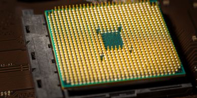
Nexus Nanoworks offers truly bespoke microfabrication with a focus on MEMS fabrication. Our hands-on expertise spans all major MEMS process categories, enabling us to customize fabrication workflows to meet the unique materials, structures, and performance requirements of each project.
Many facilities face challenges with flexibility in material systems, consistency in contamination control, or they tend to shy away from process consulting outside their established workflows. Nexus Nanoworks was specifically designed to excel in this area. We provide robust microelectronics support for unconventional processes, novel materials, and technically complex fabrication paths with precision and control.
Process Consulting
Process Consulting
Process Consulting

Nexus Nanoworks offers expert process consulting for microelectronics support, specializing in microelectronics, MEMS fabrication, and nano-scale fabrication workflows. We assist clients with process definition, refinement, and validation across lithography, thin films, etch, and integration, whether enhancing an existing flow or developing one from the ground up.
Our consulting emphasizes practical, fabrication-aware guidance, including DFM, contamination control, stress management, yield improvement, and troubleshooting process failures. We collaborate closely with engineering teams to translate concepts into repeatable, manufacturable processes suitable for prototyping, pilot production, and technology transfer.
Design
Process Consulting
Proposal Support

Nexus Nanoworks provides comprehensive microelectronics support to clients at every stage of development, from early concepts to the refinement of existing designs and processes. Whether you're starting from a preliminary idea or an established MEMS fabrication flow, we offer the experience needed to translate designs into functional, manufacturable devices.
Our team has extensive experience in mask and reticle design for MEMS and microelectronics, covering everything from simple device structures to complex, multi-layer layouts. In addition to design execution, we provide valuable process consulting, assisting with process definition, tool selection, and cleanroom planning. We draw on practical experience across multiple fabrication environments to ensure designs are efficient, realistic, and buildable.
Proposal Support
Proposal Support
Proposal Support

Nexus Nanoworks provides hands-on support for technical proposal development, specifically in the field of MEMS fabrication and microelectronics support. We help teams translate complex engineering and scientific work into clear, competitive submissions. Collaborating closely with clients, we strengthen technical narratives while ensuring accuracy, depth, and relevance to reviewers.
Our support encompasses drafting and refining proposal responses, enhancing structure and clarity, tightening technical arguments, and addressing common reviewer concerns. Our process consulting approach focuses on producing proposals that are coherent, focused, and aligned with stated evaluation criteria, all while preserving technical depth.
Grant Consulting
Proposal Support
Grant Consulting

Nexus Nanoworks offers grant consulting services that focus on program alignment and strategic positioning, specifically for MEMS fabrication and microelectronics support. We help identify appropriate funding opportunities while ensuring that proposed technical work aligns with program goals, priorities, and review frameworks.
Our consulting emphasizes early-stage guidance, including program fit assessment, scope alignment, and strategic framing to enhance competitiveness. We support research, manufacturing, and commercialization-focused programs, providing process consulting that helps teams position their work clearly and realistically for funding success.
How We Work
Proposal Support
Grant Consulting

Nexus Nanoworks serves as a collaborative technical partner, engaging closely with clients from initial discussion through execution and review. We start by understanding project goals, material constraints, and technical risks, then outline a practical path forward that reflects real fabrication conditions rather than idealized assumptions, especially in the context of MEMS fabrication.
Our work is conducted across established microfabrication and research laboratories in New York State, providing access to advanced tools and specialized processes. This flexible lab model supports iterative development, focused prototyping, and process refinement while delivering microelectronics support. We prioritize clear communication, disciplined process control, and realistic timelines, ensuring that our clients receive comprehensive process consulting throughout their projects.
ADditonal Capabilities

Lithography & Patterning
Our microelectronics support includes comprehensive photolithography process assistance, which encompasses photoresist (PR) coating, soft bake, post-application bake, post-exposure bake, hard bake, development, and mask/reticle integration, all essential for MEMS fabrication and process consulting.
Thin Films & Deposition
Thin-film process development for MEMS fabrication encompasses various techniques such as PECVD, LPCVD, PVD, sputtering, and thermal evaporation, alongside thermal oxidation. This includes essential aspects like stress tuning, tensile/compressive stress control, and the creation of low-stress silicon nitride (SiN) and silicon dioxide films, all of which are crucial for effective microelectronics support and process consulting.
Etch & Plasma Processing
Our expertise in MEMS fabrication includes process development and troubleshooting for RIE, DRIE, ICP, and ICP-RIE, ensuring optimal precision in micro- and nano-scale pattern transfer and material selectivity, while providing essential microelectronics support and process consulting.
Inspection, Metrology & Quality Control
Device inspection and failure analysis for MEMS fabrication and microelectronics support using optical microscopy, SEM, TEM, X-ray, EDX/EDAX, and morphology assessment to aid in process consulting, validation, and quality control.
Device Singulation & Handling
We offer comprehensive support for MEMS fabrication, including stealth dicing, singulation strategies, grid handling, and post-fabrication device preparation, alongside expert microelectronics support and process consulting.
Organic Electronics & Encapsulation
We provide process support for organic electronics, including organic encapsulation, photodiodes, and hybrid material systems that require contamination control and specialized handling. Our expertise extends to MEMS fabrication and comprehensive microelectronics support, as well as process consulting to optimize these technologies.
Prototyping & Troubleshooting
We offer rapid prototyping, process consulting, and troubleshooting to enhance the repeatability of custom microelectronics, MEMS fabrication, and system-on-a-chip devices.
U.S.-Based Fabrication Support
All work is performed in New York State, operating within the state’s growing nanotechnology and semiconductor corridor, while providing MEMS fabrication and microelectronics support, and contributing to U.S.-based, Made-in-USA development and manufacturing initiatives through process consulting.
And More!
Our capabilities extend beyond this list. If your project involves specialized materials, non-standard processes, or emerging fabrication challenges, particularly in the realm of MEMS fabrication or microelectronics support, we encourage you to reach out for process consulting to discuss feasibility.